Tag: Lam Research

  • BESI: The $15 Billion Chess Move – Hybrid Bonding and the M&A Surge

    BESI: The $15 Billion Chess Move – Hybrid Bonding and the M&A Surge

    Date: 3/13/2026

    Introduction

    On March 13, 2026, the European semiconductor landscape was jolted by a 10.2% surge in shares of BE Semiconductor Industries (Euronext Amsterdam: BESI), as rumors of a high-stakes bidding war reached a fever pitch. Reports circulating in financial centers from Amsterdam to Santa Clara suggest that industry giants Lam Research (NASDAQ: LRCX) and Applied Materials (NASDAQ: AMAT) are both exploring multi-billion-euro offers for the Dutch assembly equipment leader.

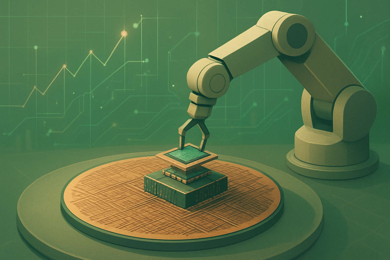
    The catalyst for this sudden move is no mystery: BESI has successfully positioned itself as the "tollgate" for the next generation of artificial intelligence (AI) hardware. With the semiconductor industry hitting the physical limits of traditional transistor shrinking, the focus has shifted to "Advanced Packaging." BESI’s mastery of hybrid bonding—a process essential for the 3D-stacking of High Bandwidth Memory (HBM4) and high-performance chiplets—has transformed it from a niche back-end player into a strategic asset of global consequence. Today’s market action reflects a growing realization that BESI is no longer just an equipment supplier; it is the linchpin of the 2026 AI infrastructure boom.

    Historical Background

    BE Semiconductor Industries, commonly known as Besi, was founded in May 1995 by Richard Blickman. The company’s roots trace back to the assembly equipment division of Philips Semiconductors and the early days of ASM International. Since its inception, Besi has been led by Blickman, whose tenure of over 30 years makes him one of the longest-serving and most respected CEOs in the European tech sector.

    In its first decade, Besi focused on traditional "back-end" tools—die attach, packaging, and plating—where it competed on reliability and cost. However, a series of strategic acquisitions in the mid-2000s, including Datacon (2005) and ESEC (2010), allowed the company to pivot toward higher-precision technologies like flip-chip and thermo-compression bonding (TCB). This evolution was not just about scale but about foresight; Blickman correctly anticipated that as "More than Moore" scaling took hold, the "back-end" of chip manufacturing would eventually require the same atomic-level precision as the "front-end." This transformation culminated in the early 2020s with Besi’s breakthrough into hybrid bonding, solidifying its place at the top of the value chain.

    Business Model

    Besi operates a high-margin, specialized business model focused on the assembly and packaging of semiconductor devices. Unlike diversified rivals, Besi concentrates on high-end niche segments where technical requirements are most demanding.

    The company’s revenue is categorized into three primary product lines:

    1. Die Attach Equipment (Lead segment): High-precision systems that place individual silicon chips onto substrates or other chips. This includes their flagship hybrid bonding and TCB systems.
    2. Packaging Equipment: Systems for molding and trim-and-form processes that protect the silicon die.
    3. Plating Equipment: Equipment used for the chemical processing of semiconductor leads and connectors.

    Besi’s customer base includes the world’s leading foundries and IDMs (Integrated Device Manufacturers), such as TSMC, Intel, and Samsung, as well as outsourced semiconductor assembly and test (OSAT) providers like ASE and Amkor. By focusing on the highest-complexity tools, Besi maintains industry-leading gross margins, often exceeding 60%—a rarity in the traditionally low-margin assembly equipment sector.

    Stock Performance Overview

    Besi has been a "multibagger" for long-term investors, outperforming the broader SOX (PHLX Semiconductor Sector) index over multiple time horizons.

    • 10-Year Horizon (2016–2026): Besi has delivered a staggering cumulative return of over 1,500%. Notable growth spurts occurred in 2017 (driven by smartphone 3D-sensing) and 2023 (the GenAI breakthrough).
    • 5-Year Horizon (2021–2026): Despite the post-pandemic "chip glut" of 2022, the stock recovered and surged as the market shifted focus from consumer electronics to AI data centers.
    • 1-Year Horizon: Over the past 12 months, the stock has risen 41%, significantly buoyed by Applied Materials taking a 9.2% strategic stake in April 2025.
    • Today (3/13/2026): The 10% jump has pushed the stock to a record high of ~€235, bringing its market capitalization to approximately €15.5 billion.

    Financial Performance

    In its most recent FY 2025 earnings report (released February 2026), Besi demonstrated remarkable resilience. While the automotive and mobile sectors remained sluggish, AI-related orders provided a massive tailwind.

    • Revenue: €591.3 million (FY 2025), a slight dip from 2024 but masking a strong H2 recovery.
    • Gross Margin: 63.3%, maintaining its status as a high-rent tech leader.
    • Order Backlog: A record H2 2025, where orders surged by 63.6% compared to H1, primarily driven by early bookings for HBM4 production lines.
    • Cash Flow & Debt: Besi maintains a "fortress balance sheet" with significant net cash and a consistent history of returning capital to shareholders via dividends and buybacks, making it an attractive acquisition target for cash-rich US firms.

    Leadership and Management

    Richard Blickman’s leadership is synonymous with Besi’s success. His strategy has centered on three pillars: R&D leadership, cost flexibility (using a "flexible production" model in Malaysia), and a disciplined M&A approach.

    Under Blickman, Besi has avoided the "diworsification" that plagued some of its larger peers. The management team is known for its conservative financial guidance and exceptional operational execution. However, as of early 2026, succession planning has become a topic of conversation among institutional investors, given Blickman's long tenure. This perceived "transition risk" may be one reason why the board is reportedly open to discussing a merger with a larger entity that could provide a more institutionalized corporate structure.

    Products, Services, and Innovations

    The crown jewel of Besi’s portfolio is the Kinex™ Hybrid Bonding system, developed in partnership with Applied Materials.

    • Hybrid Bonding: Unlike traditional methods that use solder "bumps" to connect chips, hybrid bonding uses direct copper-to-copper bonds at a pitch of less than 5 microns. This allows for 1,000x more interconnects between chips, reducing power consumption by 20% and increasing data transfer speeds exponentially.
    • HBM4 Integration: As the memory industry moves toward HBM4 in 2026-2027, Besi’s tools are the only ones capable of the sub-micron accuracy required to stack 16 or 24 layers of memory dies.
    • Innovation Pipeline: Besi is currently testing "Laser-Assisted Bonding" (LAB) and advanced TCB solutions for next-gen automotive sensors, ensuring they remain relevant as electric vehicle (EV) chip content grows.

    Competitive Landscape

    Besi competes in a consolidated but fiercely competitive market.

    • ASMPT (ASM Pacific Technology): Besi’s largest rival. While ASMPT has a broader portfolio and larger scale, it has traditionally struggled to match Besi’s precision in the ultra-high-end hybrid bonding segment.
    • Kulicke & Soffa (NASDAQ: KLIC): The leader in traditional wire bonding. K&S has attempted to move into advanced packaging (TCB), but is viewed more as a mid-range provider compared to Besi’s "high-performance" focus.
    • Hanmi Semiconductor: A Korean specialist that has dominated the "Dual-TC" bonding market for HBM3e, posing a significant threat in the memory sub-segment.

    The competitive advantage for Besi lies in its deep integration with front-end toolmakers (specifically AMAT), which creates a "moat" that is difficult for pure back-end players to cross.

    Industry and Market Trends

    The semiconductor industry in 2026 is defined by "Front-end and Back-end Convergence."
    As chiplets become the standard architecture for AI processors (like those from NVIDIA and AMD), the distinction between making a chip and assembling it is blurring. Packaging now requires cleanroom environments and chemical mechanical planarization (CMP)—technologies usually found in wafer fabs. This trend is the primary driver behind the interest from Lam Research and Applied Materials; both companies want to own the entire "stack" of manufacturing to capture the value created by multi-die integration.

    Risks and Challenges

    Despite its dominance, Besi faces several critical risks:

    1. Geopolitical Regulation: The Dutch government’s "Vifo Act" allows for the blocking of foreign acquisitions of sensitive technology. A US buyout of a Dutch champion could face significant political resistance in the Hague and Brussels.
    2. Cyclicality: Despite the AI boom, Besi remains exposed to the highly cyclical mobile and automotive markets, which can lead to volatile quarterly earnings.
    3. Technology Delay: If memory makers (SK Hynix, Samsung) decide to stick with cheaper TCB methods for longer than expected, the adoption ramp for Besi’s expensive hybrid bonders could be delayed.

    Opportunities and Catalysts

    • M&A Bidding War: The most immediate catalyst is the potential for a bidding war. With AMAT already owning nearly 10%, Lam Research may need to offer a significant premium (estimated at €270-€300 per share) to wrest control.
    • HBM4 Standardization: As JEDEC (the standards body) finalizes HBM4 specifications in late 2026, a surge in capital expenditure from memory makers is expected.
    • Expansion into Glass Substrates: Besi is rumored to be working with Intel on glass substrate bonding, a technology that could replace organic substrates in the late 2020s.

    Investor Sentiment and Analyst Coverage

    Sentiment among institutional investors is overwhelmingly bullish. BlackRock and Capital Group remain the largest shareholders, and analyst ratings as of March 2026 show 18 "Buys," 4 "Holds," and 0 "Sells."

    Retail chatter on platforms like X and Reddit has surged alongside today’s price action, with many "AI-pure-play" investors viewing Besi as the "ASML of the back-end." The consensus among Wall Street analysts is that Besi is a "must-own" for any fund focused on the physical layer of the AI revolution.

    Regulatory, Policy, and Geopolitical Factors

    The Dutch "Vifo Act" (Investments, Mergers, and Acquisitions Security Screening Act) is the primary hurdle for any potential acquisition. The Netherlands is increasingly protective of its semiconductor ecosystem, which includes ASML, NXP, and Besi. However, given that Applied Materials is already a strategic partner and the US is a key security ally, a deal might be structured with "sovereignty guarantees"—ensuring R&D and jobs remain in the Netherlands—to appease regulators. Furthermore, the EU Chips Act encourages local champions to scale, which could ironically lead to more openness toward US capital if it strengthens the European ecosystem's global standing.

    Conclusion

    The 10% surge in Besi’s stock on March 13, 2026, marks a pivotal moment in the "Advanced Packaging" era. Whether Besi remains an independent Dutch champion or becomes a subsidiary of a Silicon Valley titan like Applied Materials or Lam Research, its technology is now undeniably essential.

    For investors, the BESI story is no longer about the "back-end" of the chip industry; it is about the fundamental architecture of the AI future. While the regulatory road to a merger may be long and fraught with political sensitivity, the strategic logic is clear: in a world of multi-die chiplets and HBM4, Besi holds the keys to the kingdom. Investors should watch for formal filings from the Dutch AFM (Authority for the Financial Markets) regarding ownership thresholds, as any move past 10% by Lam or AMAT could trigger a mandatory offer and redefine the semiconductor landscape for the next decade.


    This content is intended for informational purposes only and is not financial advice.

  • The Architecture of AI: A Deep Dive into Lam Research (LRCX) and the Advanced Packaging Revolution

    The Architecture of AI: A Deep Dive into Lam Research (LRCX) and the Advanced Packaging Revolution

    Date: February 9, 2026

    Introduction

    As the global economy grapples with the transformative shifts of the mid-2020s, the "AI gold rush" has moved beyond the chip designers and into the ultra-precise world of semiconductor manufacturing equipment. At the heart of this transition is Lam Research (Nasdaq: LRCX), a Silicon Valley stalwart that has reinvented itself from a cyclical memory-play into an indispensable architect of the AI infrastructure age.

    While the limelight often focuses on the high-powered GPUs designed by firms like NVIDIA (Nasdaq: NVDA), the physical manifestation of these chips—specifically the "advanced packaging" that allows them to process massive datasets at lightning speeds—is where Lam Research has staked its claim. As of early 2026, the demand for High Bandwidth Memory (HBM) and 2.5D/3D chip stacking has reached a fever pitch, placing Lam’s specialized etching and deposition tools at the very center of the global technology supply chain.

    Historical Background

    Founded in 1980 by Dr. David K. Lam, the company initially focused on plasma etching—a process of removing material from a silicon wafer to create the intricate patterns that form a transistor. By the 1990s, Lam had established itself as a leader in the etch market, but its path was not without volatility. The company faced near-collapse during the dot-com bubble burst, necessitating a radical restructuring.

    The 2010s marked a period of strategic consolidation and expansion. Under the leadership of former CEO Steve Newberry and current CEO Tim Archer, Lam expanded its portfolio through the acquisition of Novellus Systems in 2012, which added crucial deposition capabilities. This move transformed Lam into a multi-product powerhouse, capable of handling both the "subtractive" (etching) and "additive" (deposition) phases of chipmaking. This synergy is exactly what has allowed the company to dominate the current advanced packaging market, where layers must be added and etched with atomic-level precision.

    Business Model

    Lam Research operates under a robust, two-pronged business model. The first is System Sales, where the company sells its high-margin wafer fabrication equipment (WFE) to leading foundries and memory manufacturers. This segment is highly sensitive to the capital expenditure cycles of giants like TSMC, Samsung, and Intel.

    The second, and increasingly vital, component is the Customer Support Business Group (CSBG). As the installed base of Lam’s machines grows, the company generates recurring revenue through spare parts, maintenance services, and equipment upgrades. In the 2025 fiscal year, CSBG acted as a critical stabilizer, providing high-margin, predictable cash flows even when the broader equipment market faced geopolitical headwinds. Lam’s "service-led" model ensures that once a tool is placed on a factory floor, it generates revenue for 15 to 20 years.

    Stock Performance Overview

    Investors who recognized Lam’s pivot toward AI infrastructure early have been handsomely rewarded. As of February 2026, the stock’s performance metrics are a testament to its market dominance:

    • 1-Year Performance: The stock is up approximately 179% over the past twelve months, fueled by the unexpected acceleration of HBM4 development and the broadening of AI into edge computing.
    • 5-Year Performance: On a split-adjusted basis, LRCX has seen a 333% increase. The company’s successful navigation of the post-pandemic supply chain crisis and the 2023 memory downturn solidified investor confidence.
    • 10-Year Performance: Over the last decade, Lam Research has delivered a staggering total return of ~3,730%, outperforming the S&P 500 and most of its peers in the PHLX Semiconductor Sector (SOX) index.

    The stock hit a record high of $248.17 in January 2026, followed by a period of healthy consolidation as the market digested a flurry of earnings reports.

    Financial Performance

    Lam’s financial health in early 2026 is at an all-time peak. For the fiscal year 2025, the company reported revenue of $18.44 billion, a 23.7% increase from the previous year. The most recent quarterly results (Q2 FY2026, ended December 2025) saw revenue hit $5.34 billion, comfortably beating analyst estimates.

    Key financial metrics include:

    • Gross Margin: 49.7%, reflecting the high value of its proprietary AI-centric tools.
    • Operating Margin: 34.3%, a industry-leading figure that highlights operational efficiency.
    • Earnings Per Share (EPS): Non-GAAP EPS rose 39.6% year-over-year to $1.27 (post-split).
    • Capital Allocation: The company has remained aggressive with its buyback program, returning over $3 billion to shareholders in 2025, alongside a steadily increasing dividend.

    Leadership and Management

    CEO Tim Archer, who took the helm in late 2018, is widely credited with the "Velocity" strategy—a focus on reducing the time it takes for new semiconductor technologies to reach high-volume manufacturing. Archer’s background in engineering and his tenure as COO have given him a unique "under-the-hood" understanding of the company's technical moats.

    In response to the unprecedented demand for advanced packaging, Archer recently reorganized the executive suite. Sesha Varadarajan was promoted to Chief Operating Officer (COO) to oversee the scaling of manufacturing for the Akara and Syndion platforms. This leadership team is viewed by Wall Street as highly disciplined, with a reputation for meeting or exceeding guidance through multiple industry cycles.

    Products, Services, and Innovations

    The "secret sauce" of Lam’s recent success lies in its Advanced Packaging solutions. As traditional "front-end" scaling (making transistors smaller) becomes exponentially more expensive, the industry has turned to "back-end" innovation.

    • Syndion® Etch Series: This tool is the gold standard for Through-Silicon Via (TSV) etching. TSVs are the vertical connections that allow memory chips to be stacked 12, 16, or even 20 layers high in HBM4.
    • SABRE® 3D: This electroplating tool is used for copper pillar and microbump formation. It is essential for the 2.5D interposers that act as the high-speed "highway" between a GPU and its memory.
    • Akara™ Platform: Launched in 2024 and scaled in 2025, Akara combines etch and deposition into a single, high-throughput environment designed specifically for the extreme aspect ratios of next-generation AI chips.

    These innovations have protected Lam’s market share, particularly as the "content per wafer" for AI chips is significantly higher than for standard server or PC chips.

    Competitive Landscape

    Lam Research operates in a concentrated market where barriers to entry are immense. Its primary rivals include:

    • Applied Materials (Nasdaq: AMAT): The largest equipment maker by total revenue. While AMAT leads in Chemical Mechanical Planarization (CMP), Lam remains the preferred choice for the most difficult high-aspect-ratio etch applications.
    • Tokyo Electron (Tokyo: 8035): A formidable Japanese competitor with a strong foothold in the Asian supply chain. TEL is currently investing heavily in its own advanced packaging hubs to challenge Lam’s etch dominance.
    • ASML (Nasdaq: ASML): While ASML dominates lithography, it does not compete directly in etch or deposition. However, the two companies are highly symbiotic; ASML prints the patterns, and Lam carves them.
    • BE Semiconductor Industries (Euronext: BESI): Known as "Besi," this company leads in hybrid bonding, the final step where two chips are fused together. Lam’s tools are the critical precursors that prepare the wafers for Besi’s bonding process.

    Industry and Market Trends

    The semiconductor industry is currently defined by three major trends:

    1. Heterogeneous Integration: Combining different types of chips (CPUs, GPUs, HBM) into a single package to maximize performance.
    2. HBM4 Transition: The shift from HBM3e to HBM4 is requiring a complete overhaul of the manufacturing process, favoring companies like Lam that provide the tools for 16-high stacks.
    3. Regionalization: Prompted by geopolitical tensions, countries are subsidizing "sovereign" semiconductor supply chains. The U.S. CHIPS Act and similar initiatives in Europe and Japan have led to a massive construction boom in new fabs, all of which require Lam’s equipment.

    Risks and Challenges

    Despite its strengths, Lam Research is not without risk.

    • China Exposure: China accounted for roughly 34% of Lam’s revenue in 2025. While a temporary "truce" in late 2025 allowed for some sales of modified AI tools, the threat of renewed export bans or reciprocal tariffs remains a significant overhang on the stock.
    • Cyclicality: While AI has dampened the traditional semiconductor cycle, the industry remains prone to periods of oversupply. If AI demand were to cool unexpectedly, Lam’s order book could shrink rapidly.
    • R&D Costs: Maintaining its technical moat requires billions in annual research spending. Any failure to innovate in the next generation of atomic layer etching (ALE) could cede market share to Tokyo Electron or Applied Materials.

    Opportunities and Catalysts

    Looking ahead, several catalysts could drive further growth:

    • GAA (Gate-All-Around) Transistors: As logic chips move to 2nm and below, the transition from FinFET to GAA transistors will require significantly more etching and deposition steps, directly benefiting Lam.
    • Backside Power Delivery: A new chip architecture that moves power wires to the back of the wafer to reduce congestion. This requires specialized etching that Lam is currently pioneering.
    • M&A Activity: With a strong cash position, Lam is well-positioned to acquire smaller players in the metrology or inspection space to broaden its "all-in-one" solution for chipmakers.

    Investor Sentiment and Analyst Coverage

    Wall Street remains broadly bullish on LRCX. As of February 2026, over 75% of analysts covering the stock maintain a "Buy" or "Strong Buy" rating. Hedge fund interest has also spiked, with institutional ownership nearing 85%.

    Retail sentiment is equally positive, often viewing Lam as a "pick and shovel" play that is safer than individual chip designers. However, some value-oriented investors have raised concerns about its current valuation, which sits at a forward P/E ratio of approximately 28x—a premium compared to its historical average of 18-22x.

    Regulatory, Policy, and Geopolitical Factors

    The regulatory landscape in 2026 is complex. The U.S. government’s "25% Arrangement" for China—whereby companies can sell certain technologies in exchange for a portion of the revenue going to federal coffers—has created a complicated compliance environment.

    Additionally, the expiration of several "temporary" export licenses in November 2026 is a date investors are watching closely. Any escalation in the trade war between the U.S. and China would hit Lam harder than many of its peers due to its large footprint in the Chinese "legacy" chip market, which remains the primary driver of its older-generation tool sales.

    Conclusion

    Lam Research stands as a quintessential beneficiary of the AI era. By dominating the critical etching and deposition steps required for advanced packaging and HBM4, the company has transformed from a cyclical equipment provider into a structural growth story. While geopolitical tensions and a rich valuation present real risks, Lam’s technical moats and disciplined management make it a foundational holding for anyone seeking exposure to the physical infrastructure of artificial intelligence. Investors should keep a close eye on the November 2026 regulatory deadline and the progress of the Akara platform as indicators of the company's long-term trajectory.


    This content is intended for informational purposes only and is not financial advice.

  • Lam Research (LRCX) Deep-Dive: Architecture of the AI Supercycle

    Lam Research (LRCX) Deep-Dive: Architecture of the AI Supercycle

    Date: January 23, 2026

    Introduction

    As the semiconductor industry navigates the most significant technological pivot since the invention of the integrated circuit, few companies sit at a more critical juncture than Lam Research (Nasdaq: LRCX). Often described as a "picks and shovels" play for the digital age, Lam provides the high-precision equipment required to etch and deposit the microscopic layers that form modern microchips. Following a resounding "Q3" earnings beat (referring to the most recent fiscal reporting cycle that exceeded Wall Street expectations) and an exceptionally bullish outlook for the semiconductor equipment sector, Lam Research has become the centerpiece of the investor conversation surrounding AI infrastructure.

    With today's date of January 23, 2026, the company finds itself at the heart of a "supercycle" driven by High Bandwidth Memory (HBM) and the transition to Gate-All-Around (GAA) transistor architectures. This article provides an in-depth look at the mechanics of Lam Research, its strategic leadership, and why it remains a foundational pillar for the next decade of computing.

    Historical Background

    Lam Research was founded in 1980 by Dr. David K. Lam, a Chinese-born engineer who recognized a glaring gap in the nascent chip industry: the need for automated, precise etching. Before Lam, etching—the process of removing material from a silicon wafer to create circuit patterns—was often a messy, manual process. Dr. Lam introduced the Plasma Etch system, which brought a new level of repeatability and precision to the cleanroom.

    The company went public in 1984, but its true transformation occurred in the early 2010s. By acquiring Novellus Systems in 2012 for $3.3 billion, Lam Research expanded from its dominance in "Etch" to become a powerhouse in "Deposition" (the process of adding layers of material). This merger created a comprehensive toolset that allowed chipmakers to partner with a single vendor for the most difficult "atomic-level" manufacturing steps. Over the last decade, Lam has evolved from a cyclical hardware vendor into a specialized technology partner essential for the fabrication of 3D NAND and advanced logic chips.

    Business Model

    Lam Research operates a highly lucrative and defensible business model centered on two primary segments:

    1. Semiconductor Manufacturing Systems: This segment accounts for the majority of revenue, involving the sale of high-cost tools like the Kiyo (etching), Vector (deposition), and Sabre (electroplating) product lines. These machines can cost tens of millions of dollars each and are essential for companies like TSMC, Intel, and Samsung.
    2. Customer Support Business Group (CSBG): This is Lam’s "razor and blade" strategy. Once a tool is installed, it requires specialized parts, services, and software upgrades. This segment provides a recurring revenue stream that is less volatile than tool sales, often accounting for 30-40% of total revenue. As the installed base of Lam machines grows, this high-margin service business expands, providing a floor for earnings during industry downturns.

    Lam's customer base is concentrated among the world's top semiconductor manufacturers, making its relationships deep, integrated, and difficult for competitors to displace.

    Stock Performance Overview

    Over the last decade, LRCX has been a standout performer in the S&P 500, significantly outperforming the broader tech sector.

    • 10-Year Horizon: Investors who held LRCX through the mid-2010s have seen massive gains, as the stock rode the wave of the smartphone revolution and the early cloud migration.
    • 5-Year Horizon: The last five years have been defined by the AI explosion. Lam’s stock price has benefited from a 10-for-1 stock split in late 2024, which increased liquidity and retail accessibility.
    • 1-Year Horizon: In the past 12 months, the stock has rallied over 45%, driven by the recovery in the memory market and the insatiable demand for HBM tools. As of January 2026, the stock is trading near all-time highs, reflecting a market that is pricing in a multi-year growth runway for AI hardware.

    Financial Performance

    The most recent earnings report, which investors are currently digesting, showcased Lam’s operational efficiency.

    • Revenue Growth: In the most recently reported quarter, Lam posted revenue of $5.32 billion, a 27.7% increase year-over-year.
    • Profitability: The company maintains robust gross margins of roughly 47-48%, a testament to its pricing power and the specialized nature of its equipment. Non-GAAP EPS came in at $1.26 (post-split), comfortably beating the $1.22 analyst consensus.
    • Balance Sheet: With over $5 billion in cash and a disciplined debt profile, Lam has the flexibility to fund massive R&D while returning capital to shareholders. The company recently increased its quarterly dividend and continues to execute a multi-billion dollar share repurchase program.

    Leadership and Management

    Under the leadership of President and CEO Tim Archer, who took the helm in late 2018, Lam Research has pivoted toward "Equipment Intelligence." Archer, a veteran of the industry with decades of experience at Novellus and Lam, has focused on integrating AI and machine learning into the tools themselves.

    The strategy—often called the "Semiverse"—aims to use digital twins and AI-driven simulation to speed up the development of new manufacturing processes. This reduces the time it takes for customers to reach high-volume production. Archer is widely respected on Wall Street for his conservative guidance and his ability to navigate the complex geopolitical landscape of semiconductor export controls.

    Products, Services, and Innovations

    Lam’s competitive edge lies in its ability to manipulate matter at the atomic scale. Key innovations include:

    • High Aspect Ratio (HAR) Etching: As memory chips move to 300+ layers of 3D NAND, the "holes" that need to be etched become incredibly deep and narrow. Lam’s Kiyo systems are the only tools capable of maintaining the precision required for these structures.
    • SABER 3D: Essential for Advanced Packaging and High Bandwidth Memory (HBM). This tool enables the "stacking" of chips, which is the current bottleneck in AI GPU production.
    • Vantex Etch: A newer platform designed specifically for the transition to 2nm and 3nm logic nodes, providing the extreme selectivity needed for Gate-All-Around (GAA) transistors.

    Competitive Landscape

    Lam Research operates in a "co-opetition" environment with other giants of the Wafer Fabrication Equipment (WFE) space:

    • Applied Materials (Nasdaq: AMAT): The largest overall rival, with a broader portfolio but less specialized dominance in etching.
    • ASML (Nasdaq: ASML): While ASML dominates lithography, Lam’s etch and deposition tools "follow" the lithography step. The two companies are more partners in the ecosystem than direct rivals.
    • Tokyo Electron (8035.T): Lam’s primary competitor in the etching space.

    Lam’s moat is built on its "Process Proximity," where its etch and deposition tools work in a closed loop to provide better results than mixing and matching tools from different vendors.

    Industry and Market Trends

    The semiconductor industry is shifting from a mobile-centric era to an AI-centric era. This has three major implications for Lam:

    1. Complexity Gain: Moving from 5nm to 2nm chips requires roughly 20% more process steps. More steps mean more Lam machines.
    2. The Memory Recovery: After a brutal downturn in 2023-2024, the NAND and DRAM markets are recovering. Lam is more exposed to memory than some of its peers, making it a primary beneficiary of this cyclical upturn.
    3. HBM Demand: AI servers require 3x more HBM than traditional servers. Lam’s equipment is vital for the advanced packaging that makes HBM possible.

    Risks and Challenges

    No investment is without risk. For Lam Research, the primary concerns are:

    • Geopolitical Friction: A significant portion of Lam’s revenue still comes from China. While the company has complied with U.S. export controls, further restrictions on older "legacy" nodes could hurt the bottom line.
    • Cyclicality: Despite the AI tailwind, the semiconductor industry remains inherently cyclical. A global macro slowdown could lead chipmakers to defer multi-billion dollar capital expenditures.
    • Innovation Risk: If a competitor develops a significantly better way to etch 3D structures (e.g., using a non-plasma method), Lam’s dominant market share could be threatened.

    Opportunities and Catalysts

    • 2nm Transition: As TSMC and Intel move into high-volume 2nm production in 2026, Lam is expected to see a "step-function" increase in tool demand.
    • Backside Power Delivery: A new chip architecture that moves power wiring to the back of the wafer. This requires intensive new etch and deposition steps, a "sweet spot" for Lam.
    • The "Silicon Forest" Expansion: Lam’s new R&D and manufacturing facilities in Oregon are coming online, allowing for faster prototyping and delivery to domestic U.S. customers under the CHIPS Act.

    Investor Sentiment and Analyst Coverage

    Sentiment among institutional investors is currently at a multi-year high. Following the recent "beat and raise," major firms like Stifel and Wells Fargo have raised their price targets to the $240-$260 range. Analysts are particularly impressed by Lam's ability to maintain high margins despite the R&D costs associated with new nodes. On retail platforms, the 2024 stock split is still viewed as a major positive, having opened the door for more fractional and retail ownership.

    Regulatory, Policy, and Geopolitical Factors

    The U.S. CHIPS and Science Act continues to be a tailwind, as it incentivizes the building of fabrication plants (fabs) in the United States. Every new fab built by Intel, Samsung, or TSMC on U.S. soil represents a massive order book for Lam Research. However, the company must balance this with the ongoing "Chip War" with China. Lam has aggressively diversified its supply chain to Southeast Asia and increased its footprint in South Korea and Taiwan to mitigate the risk of a single-point failure in the event of further trade escalations.

    Conclusion

    Lam Research is no longer just a cyclical chip-equipment company; it has matured into a vital architect of the AI era. Its dominance in etching and deposition makes it indispensable to the production of the world’s most advanced processors and memory chips.

    While geopolitical risks and the inherent cycles of the tech industry require a cautious eye, the fundamental demand for "more bits and faster logic" shows no signs of slowing down. For investors, Lam Research represents a high-quality, high-margin way to gain exposure to the physical reality of the AI revolution. As we look toward the remainder of 2026, the key metric to watch will be the pace of the NAND recovery and the successful ramp-up of 2nm production—both of which currently look like strong tailwinds for this Silicon Valley stalwart.


    This content is intended for informational purposes only and is not financial advice.